

PRODUCTS

KLA Zeta 3D Optical Imaging and Metrology System
KLA Zeta precision metrology systems that analyze high-roughness, low-reflectance surfaces for Biotech, solar cell, LED, MEMS and other micron-scale measurement applications. Our wide-field optical profilers can measure high-aspect-ratio features from the millimeter to sub-micron range, and film thicknesses down to 30nm. The bundled Zeta 3D imaging software produces true-color 3D feature maps in a fraction of the time of other surface profilers. With available Nomarski / Quantitative-DIC and Film Thickness Measurement options, our systems provide the widest range, highest flexibility and best value in its class.
Zeta's patented Z-DotTM technology enables researchers and production managers to create true-color, 3D images of sub-micron surface features for measurement applications in High-Brightness LEDs, Solar Cells, Biotech, and Magnetic Storage Media. The Z-Dots enable the system software to rapidly identify features within the plane of focus to create accurate 3D surface maps of Patterned Sapphire Substrates, Surface Textures, Microfluidic Channels, and Micro-machining defects.
MULTI MODE OPTICS TECHNOLOGY
KLA Zeta Optical Profiler integrates five powerful optical metrology technologies in one fully configurable and easy-to-use system.
It images and analyzes different size features on samples of all types: smooth to rough, very low to very high reflectivity, transparent to opaque, single layer to multilayer, sub-nm to mm. The versatility of the Zeta technology is simply unmatched by any other metrology tools.
METROLOGY
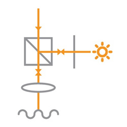
ZDot™
Zeta's proprietary 3D imaging technology combines innovative optics with powerful software algorithms to produce great results even for difficult surfaces
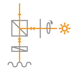
ZSI
Shearing interferometry for images with high z resolution
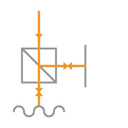 ZXI
ZXI
Interferometer optics enables wide area measurements with a high Z resolution
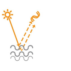
ZFT
Integrated broad-band reflectometer for thin film thickness and surface reflectance measurements
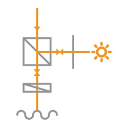
ZIC
Interference contrast technique providing enhanced & quantitative images of sub-nanometer level roughness
AOI
Automated Optical Inspection option combines Metrology and Defect Inspection into one efficient, cost effective, and powerful system
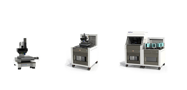
Zeta-20 Optical Profiler
The Zeta-20 is a fully integrated optical profiling microscope that provides 3D metrology and imaging capability in a compact, robust package. The system is powered by ZDot™ technology, which simultaneously collects high-resolution 3D data and a True Color infinite focus image. The Zeta-20 supports both R&D and production environments with Multi-Mode optics, easy-to-use software, and a low cost of ownership.
Zeta-300 Optical Profiler
The Zeta-300 provides 3D metrology and imaging capability, combined with an integrated isolation table and configuration flexibility to handle larger samples. The system is powered by ZDot™ technology, which simultaneously collects high-resolution 3D data and a True Color infinite focus image. The Zeta-300 supports both R&D and production environments with Multi-Mode optics, easy-to-use software, and a low cost of ownership.
Zeta-388 Optical Profiler
The Zeta-388 provides 3D metrology and imaging capability, combined with an integrated isolation table and a cassette-to-cassette wafer handling system for fully automated measurements. The system is powered by ZDot™technology, which simultaneously collects high-resolution 3D data and a True Color infinite focus image. The Zeta-388 supports both R&D and production environments with Multi-Mode optics, easy-to-use software, a low cost of ownership, and SECS/GEM communications.
APPLICATION
- Step height: 3D step height from nanometers to millimeters
- Texture: 3D roughness and waviness on smooth to very rough surfaces
- Form: 3D bow and shape
- Stress: 2D thin film stress
- Film thickness: transparent film thickness from 30nm to 100µm
- Seed layer metal reflectivity
- PI and PR film thickness
- PI and PR opening
- Plated Cu thickness
- UBM height and roughness
- RDL thickness, width and roughness
- TSV fill monitoring
- Bump height
- Bow and stress
INDUSTRIES
- LED: light emitting diodes and PSS (patterned sapphire substrates)
- Solar: photovoltaic solar cells
- Semiconductor and compound semiconductor
- Semiconductor WLCSP (wafer-level chip scale packaging)
- Semiconductor FOWLP (fan-out wafer-level packaging)
PCB (printed circuit board) and flexible PCB - MEMS: Micro-electro-mechanical systems
- Medical devices and microfluidic devices
- Data storage
- Universities, research labs and institutes
- And more: Contact us with your requirements